

Taishan Pi provides HDMI, eDP, and MIPI display interfaces. Building on the previous chapters, this lesson explains how to select a display and configure it on the board.
Video Tutorial
Lesson 5 — HDMI and eDP Displays (Chinese)
Lesson 6 — MIPI Displays (Chinese)
Preparation
Display Terminology
Pixels and Resolution
A pixel is the smallest addressable element in an image. Each pixel has a position and color or brightness information. A display controls individual pixels to form an image; higher pixel density can show finer detail.
Resolution is the number of pixels across and down a display. For example, 1920 × 1080 means 1920 horizontal pixels and 1080 vertical pixels. More pixels allow more image detail.
An LED dot matrix is a simple example. In the 8 × 8 matrix below, each LED acts as one pixel, giving a resolution of 8 × 8.
Progressive Scan
A display scans pixels from left to right, then moves to the next row, continuing from the top of the image to the bottom. This happens quickly enough for us to perceive a complete image.
Display Timing
Display timing is the main configuration needed for the eDP and MIPI examples. The vendor driver is already available; adjust its timing parameters to match the panel manufacturer's specifications. Which parameters matter?
- Active area: The visible pixel area, such as 1366 × 768.
VSYNC (vertical synchronization): Marks the start of a new frame.
Vertical total: The active height plus all vertical blanking intervals.
VSYNC width (
vsync-len): The vertical sync pulse width specified by the panel.VFP (
vfront-porch): The interval between the end of active frame data and VSYNC.VBP (
vback-porch): The interval between VSYNC and the next frame's active data.HSYNC (horizontal synchronization): Synchronizes each line of pixels.
Horizontal total: The active width plus all horizontal blanking intervals.
HSYNC width (
hsync-len): The horizontal sync pulse width specified by the panel.HFP (
hfront-porch): The interval between the end of active line data and HSYNC.HBP (
hback-porch): The interval between HSYNC and the next line's active data.
Why are these parameters needed?
HSYNC and VSYNC synchronize lines and frames.
The front and back porches allow time between active data and synchronization signals.
hsync-lenandvsync-lenset the sync pulse widths required by the panel controller.hsync-activeandvsync-activeset the active signal levels.
Different panel controllers require different timings. Use the values for your panel.
What happens if the timing is wrong?
Incorrect timing may produce a black screen with the backlight on, tearing, or distorted colors.
How is refresh rate calculated?
Refresh rate = pixel clock / (horizontal total × vertical total)
Refresh rate = pixel clock / ((active width + HSYNC width + HBP + HFP) × (active height + VSYNC width + VBP + VFP))
Refresh rate = 72300000 / ((1366 + 32 + 160 + 48) × (768 + 6 + 32 + 3))
Which display outputs does Taishan Pi support?
The original tutorial lists up to 4K for HDMI, 1K for MIPI, and 2K for eDP. It also reports a community test of 2K at 45 fps over two eDP lanes and support for mirrored dual displays.
See the datasheet for display-output capabilities:
Download: Rockchip_RK3566_Datasheet_V1.2-20220601.pdf
📌 Find it under 下载中心 → 百度网盘 → 第04章.【立创·泰山派】参考资料 → 【瑞芯微】官方资料 → Linux → RK356X → Datasheet → Rockchip_RK3566_Datasheet_V1.2-20220601.pdf.
- RK3566 has two video output channels,
Video output 0andVideo output 1, with the capabilities shown below.
- The interfaces share a display source. For mirrored output, use matching display parameters and disable unused interfaces when switching outputs.
RK3566 has one VOP with two ports, VP0 and VP1. VP0 supports features such as 4K and HDR, so HDMI uses VP0 by default. The diagram below shows the connections.
HDMI
HDMI supports hot plugging and is widely used by monitors and televisions. Unlike the eDP and MIPI examples, a connected HDMI display generally works without manual panel timing configuration.
Hardware
- See
Rockchip_RK3566_Datasheet_V1.2-20220601.pdffor the interface specifications.
Download: Rockchip_RK3566_Datasheet_V1.2-20220601.pdf
📌 Find it under 下载中心 → 百度网盘 → 第04章.【立创·泰山派】参考资料 → 【瑞芯微】官方资料 → Linux → RK356X → Datasheet → Rockchip_RK3566_Datasheet_V1.2-20220601.pdf.
- 1K (1920 × 1080p) at 120 Hz
- 4K (4096 × 2304p) at 60 Hz
- Connector location
- Taishan Pi uses a Micro HDMI connector to save board space. Use a Micro HDMI-to-HDMI adapter or cable to connect a standard HDMI display.
Software
- Disable HDMI output:
diff --git a/arch/arm64/boot/dts/rockchip/tspi-rk3566-user-v10-linux.dts b/arch/arm64/boot/dts/rockchip/tspi-rk3566-user-v10-linux.dts
index 02d183d4dc69..a94dab56a544 100755
--- a/arch/arm64/boot/dts/rockchip/tspi-rk3566-user-v10-linux.dts
+++ b/arch/arm64/boot/dts/rockchip/tspi-rk3566-user-v10-linux.dts
@@ -36,7 +36,7 @@
 // #include "tspi-rk3566-dsi-v10.dtsi"

 //【开/关】HDMI 显示屏幕配置,里面内容几乎可以不用动,如果不需要hdmi显示直接注释掉即可
-#include "tspi-rk3566-hdmi-v10.dtsi"
+// #include "tspi-rk3566-hdmi-v10.dtsi"

 //【开/关】摄像头 目前视频的是ov5695
#include "tspi-rk3566-csi-v10.dtsi"- Enable HDMI output:
diff --git a/arch/arm64/boot/dts/rockchip/tspi-rk3566-user-v10-linux.dts b/arch/arm64/boot/dts/rockchip/tspi-rk3566-user-v10-linux.dts
index 02d183d4dc69..a94dab56a544 100755
--- a/arch/arm64/boot/dts/rockchip/tspi-rk3566-user-v10-linux.dts
+++ b/arch/arm64/boot/dts/rockchip/tspi-rk3566-user-v10-linux.dts
@@ -36,7 +36,7 @@
 // #include "tspi-rk3566-dsi-v10.dtsi"

 //【开/关】HDMI 显示屏幕配置,里面内容几乎可以不用动,如果不需要hdmi显示直接注释掉即可
-//#include "tspi-rk3566-hdmi-v10.dtsi"
+#include "tspi-rk3566-hdmi-v10.dtsi"

 //【开/关】摄像头 目前视频的是ov5659
#include "tspi-rk3566-csi-v10.dtsi"eDP
eDP (Embedded DisplayPort) is commonly used in laptop displays. Here we focus on configuring a panel rather than the protocol itself. Some eDP panels work with little setup; others need panel-specific timings. Taishan Pi's eDP connector is on the back of the board.
Learning Goals
- Choose a compatible display.
- Configure eDP panel timings in the device tree.
Choose a Panel
Documentation
Choose a panel with useful documentation and preferably a known working example. Ask for a reference device tree, panel timings, and any touchscreen driver. Seller support can help resolve panel-specific problems. Avoid undocumented secondhand panels, especially for your first project.
Size and Pixels
- The RK3566 datasheet lists eDP support up to 2560 × 1600 at 60 Hz. Choose a panel within the supported resolution. See
Rockchip_RK3566_Datasheet_V1.2-20220601.pdf.
Download: Rockchip_RK3566_Datasheet_V1.2-20220601.pdf
📌 Find it under 下载中心 → 百度网盘 → 第04章.【立创·泰山派】参考资料 → 【瑞芯微】官方资料 → Linux → RK356X → Datasheet → Rockchip_RK3566_Datasheet_V1.2-20220601.pdf.
- Common panel sizes include 11.6, 13.3, and 15.6 inches. Choose the size to suit your project.
Pinout
Taishan Pi uses a 30-pin, 0.5 mm-pitch eDP connector. Check the pinout, cable contact orientation, logic supply, and backlight supply before connecting a panel. Matching pin counts alone do not establish compatibility. See page 24 of the board schematic. An incompatible connection can damage the display or board. If unsure, share the panel specifications and ask for help checking compatibility before connecting it.
| Pin | Name | Description | Notes |
|---|---|---|---|
| 1 | CABC_ENIN | CABC input | Content-adaptive backlight control input; may be left unconnected. |
| 2 | H_GND | High Speed Ground | High Speed Ground |
| 3 | Lane1_N | Complement Signal Link Lane 1 | Complement Signal Link Lane 1 |
| 4 | Lane1_P | True Signal Link Lane 1 | True Signal Link Lane 1 |
| 5 | H_GND | High Speed Ground | High Speed Ground |
| 6 | Lane0_N | Complement Signal Link Lane 0 | Complement Signal Link Lane 0 |
| 7 | Lane0_P | True Signal Link Lane 0 | True Signal Link Lane 0 |
| 8 | H_GND | High Speed Ground | High Speed Ground |
| 9 | AUX_CH_P | True Signal Auxiliary Channel | True Signal Auxiliary Channel |
| 10 | AUX_CH_N | Complement Signal Auxiliary Channel | Complement Signal Auxiliary Channel |
| 11 | H_GND | High Speed Ground | High Speed Ground |
| 12 | LCD_VCC | LCD logic power (3.3V) | LCD logic power (3.3V) |
| 13 | LCD_VCC | LCD logic power (3.3V) | LCD logic power (3.3V) |
| 14 | BIST | enable | Built-in self-test enable. |
| 15 | LCD_GND | LCD Ground | LCD Ground |
| 16 | LCD_GND | LCD Ground | LCD Ground |
| 17 | HPD | HPD signal pin | HPD signal pin |
| 18 | BL_GND | Backlight ground | Backlight ground |
| 19 | BL_GND | Backlight ground | Backlight ground |
| 20 | BL_GND | Backlight ground | Backlight ground |
| 21 | BL_GND | Backlight ground | Backlight ground |
| 22 | BL_ENABLE | BL_PWR | BL_PWR |
| 23 | PWM_DIM | System PWM signal input | System PWM signal input |
| 24 | Hsync | Hsync | Hsync |
| 25 | NC | No Connection | No Connection |
| 26 | BL_PWR | Backlight | Backlight supply, commonly 5–21 V; confirm the value in the panel datasheet. |
| 27 | BL_PWR | Backlight | Backlight supply, commonly 5–21 V; confirm the value in the panel datasheet. |
| 28 | BL_PWR | Backlight | Backlight supply, commonly 5–21 V; confirm the value in the panel datasheet. |
| 29 | BL_PWR | Backlight | Backlight supply, commonly 5–21 V; confirm the value in the panel datasheet. |
| 30 | NC | No Connection | No Connection |
| 31–32 | FPC mounting pads | - | The connector has 30 signal pins; 31 and 32 are its mounting pads. |
Schematic:
Pin 1 (CABC_ENIN) is on the left in the board photo below. Check the pin functions before connecting the cable. A footprint's white dot may mark pin 30 rather than pin 1.
Panel Example
Search Taobao or 1688 for 30pin EDP. Compare the specifications, price, and seller support. Ask for a pinout; it may also be in the product listing.
The example panel was purchased for testing; the listing is a reference, with no after-sales responsibility assumed by the tutorial author. Product listing. The example panel's resolution is within the eDP limit stated above: 2560 × 1600 at 60 Hz.
Check the Pinout
Compare the panel pinout with Taishan Pi's eDP pinout.
Connect Panel
This panel connects through a 30-pin, 0.5 mm-pitch ribbon cable. Some sellers include one; otherwise, search for EDP 排线 0.5MM 30P. Check whether the exposed contacts must be on the same side or opposite sides at the two ends. The wrong cable can damage the panel or board. This example uses a same-side-contact cable.
Same-side-contact and opposite-side-contact cables:
The panel connection:
Connector orientation at each end:
Match the required pins between the board and panel. If the cable type is unclear, trace pin 1 and pin 30 through both connectors as shown. Use the contact orientation that connects the corresponding pins correctly.
For the example panel's specifications, see M116BE0049A-1366X768 EDP(TN).pdf.
Download M116BE0049A-1366X768 EDP(TN).pdf
📌 Find it under 下载中心 → 百度网盘(立创·泰山派开发板资料) → 第09章.【立创·泰山派】项目案例 → 【智能小手机】项目资料 → 5.屏幕选型与调试 → EDP屏资料 → M116BE0049A-1366X768 EDP(TN).pdf.
Configure the Panel
Open the Taishan Pi user device tree, linux/kernel/arch/arm64/boot/dts/tspi-rk3566-user-v10-linux.dts, and locate the included eDP configuration.
diff --git a/arch/arm64/boot/dts/rockchip/tspi-rk3566-user-v10-linux.dts b/arch/arm64/boot/dts/rockchip/tspi-rk3566-user-v10-linux.dts
index 97da688286b2..2c54798fcd2d 100755
--- a/arch/arm64/boot/dts/rockchip/tspi-rk3566-user-v10-linux.dts
+++ b/arch/arm64/boot/dts/rockchip/tspi-rk3566-user-v10-linux.dts
@@ -30,13 +30,13 @@
 #include "tspi-rk3566-core-v10.dtsi"

 //【开/关】EDP 显示屏幕配置,用户可以基于此复制自己的屏幕,注意EDP与MIPI屏幕互斥,因为共用了VOP如果需要同显自行修改
-// #include "tspi-rk3566-edp-v10.dtsi"
+#include "tspi-rk3566-edp-v10.dtsi"

 //【开/关】mipi 显示屏幕配置,用户可以基于此复制自己的屏幕,注意EDP与MIPI屏幕互斥,因为共用了VOP如果需要同显自行修改
 // #include "tspi-rk3566-dsi-v10.dtsi"

 //【开/关】HDMI 显示屏幕配置,里面内容几乎可以不用动,如果不需要hdmi显示直接注释掉即可
-#include "tspi-rk3566-hdmi-v10.dtsi"
+// #include "tspi-rk3566-hdmi-v10.dtsi"

 //【开/关】摄像头 目前视频的是ov5659
#include "tspi-rk3566-csi-v10.dtsi"eDP Device Tree
The eDP configuration is in tspi-rk3566-edp-v10.dtsi under the kernel's Rockchip device-tree directory. In the example below, lines 13–21 contain the panel timings. The following sections explain the other settings; beginners can first work through the panel timing example.
/ {
        edp_panel: edp-panel {
                compatible = "simple-panel";    //上节我们讲过的edp驱动通过这个来匹配设备树
                backlight = <&backlight>;   // 引用背光,在下面背光是一个PWM信号
                enable-gpios = <&gpio0 RK_PA6 GPIO_ACTIVE_HIGH>;  // 激活GPIO引脚
                enable-delay-ms = <120>;  // 开启延迟时间(毫秒)
                pinctrl-0 = <&edp_en_gpio>;  // 引脚控制器

                edp_disp_timings: display-timings {
                        native-mode = <&edp_timing0>;
                        /*开始:这一部分就是我们要调试的屏幕参数了*/
                        edp_timing0: edp_timing0 {
                                clock-frequency = <150000000>;  // 像素时钟频率
                                hactive = <1920>;  // 水平像素数
                                vactive = <1080>;  // 垂直像素数
                                hfront-porch = <150>;  // 水平前肩期
                                hsync-len = <5>;  // 水平同步长度
                                hback-porch = <5>;  // 水平后肩期
                                vfront-porch = <3>;  // 垂直前肩期
                                vsync-len = <1>;  // 垂直同步长度
                                vback-porch = <9>;  // 垂直后肩期
                                hsync-active = <0>;  // 水平同步有效状态
                                vsync-active = <0>;  // 垂直同步有效状态
                                de-active = <0>;  // DE有效状态
                                pixelclk-active = <0>;  // 像素时钟有效状态
                        };
                        /*结束:这一部分就是我们要调试的屏幕参数了*/
                };

                ports {
                        panel_in_edp: endpoint {
                                remote-endpoint = <&edp_out_panel>;  // 引用端点连接
                        };
                };
        };
        /*这是我们的背光*/
        backlight: backlight {
                compatible = "pwm-backlight";
                pwms = <&pwm4 0 25000 0>;  // PWM参数设置
                brightness-levels = <  // 亮度级别
                        0 20 20 21 21 22 22 23
                        // 其他亮度级别
                        ...
                        254 255
                >;
                default-brightness-level = <200>;  // 默认亮度级别
        };
};

&pwm4 { //背光引脚使用的是PWM4
        status = "okay";  // PWM状态为正常
};

&pinctrl {
        edp {
                edp_en_gpio: edp-en-gpio { //这个是edp对应的使能引脚
                        rockchip,pins = <0 RK_PA6 RK_FUNC_GPIO &pcfg_pull_none>;  // GPIO设置
                };
        };
};

&edp {
        status = "okay";
        force-hpd;  // 强制HPD,这里非常重要哟,因为我们硬件上面是没有去做检测的所以要强制
        ports {
                edp_out: port@1 {
                        reg = <1>;
                        #address-cells = <1>;
                        #size-cells = <0>;
                        edp_out_panel: endpoint@0 {
                                reg = <0>;
                                remote-endpoint = <&panel_in_edp>;  // 远程端点连接
                        };
                };
        };
};

&edp_phy {
        status = "okay";  // EDP PHY状态为正常
};

&route_edp {
        status = "okay";  // EDP线路状态为正常
        //注意我们前面有讲到rk3566有两个vop,我们这里就是来链接vop的,你可以选择1或者0这里我们选择0
        connect = <&vp0_out_edp>;  // 连接设置
        // connect = <&vp1_out_edp>;
};
//注意我们前面有讲到rk3566有两个vop,我们这里就是来链接vop的,你可以选择1或者0这里我们选择0
&edp_in_vp0 {
        status = "okay";  // EDP输入VP0状态为正常
};
//注意我们前面有讲到rk3566有两个vop,我们这里就是来链接vop的,我们前面选择了vp0所以这里vp1就关掉
&edp_in_vp1 {
        status = "disabled";  // 禁用EDP输入VP1
};

&edp_panel {
        status = "okay";  // 打开edp面板,这个一定要打开哟如果用edp屏幕
};Backlight Circuit
/ {
        edp_panel: edp-panel {
                compatible = "simple-panel";    //上节我们讲过的edp驱动通过这个来匹配设备树
                backlight = <&backlight>;   // 引用背光,在下面背光是一个PWM信号
        /*这是我们的背光*/
        backlight: backlight {
                compatible = "pwm-backlight";
                pwms = <&pwm4 0 25000 0>;  // PWM参数设置
                brightness-levels = <  // 亮度级别
                        0 20 20 21 21 22 22 23
                        // 其他亮度级别
                        ...
                        254 255
                        // 如果你在安卓里面调背光发现是反的可以把这个数组倒过来
                >;
                default-brightness-level = <200>;  // 默认亮度级别
        };
};

&pwm4 { //背光引脚使用的是PWM4
        status = "okay";  // PWM状态为正常
};GPIO0_C3_d can be multiplexed as PWM4. Check its alternate functions in the datasheet.
Enable Pin
/ {
        edp_panel: edp-panel {
                compatible = "simple-panel";    //上节我们讲过的edp驱动通过这个来匹配设备树
                pinctrl-0 = <&edp_en_gpio>;  // 引脚控制器
                .......
};

&pinctrl {
        edp {
                edp_en_gpio: edp-en-gpio { //这个是edp对应的使能引脚
                        rockchip,pins = <0 RK_PA6 RK_FUNC_GPIO &pcfg_pull_none>;  // GPIO设置
                };
        };
};
.......GPIO0_A6_d is a GPIO used to switch the eDP panel on or off.
Panel Timing
Panel timing values can come from several sources:
- Ask the panel supplier for a reference configuration.
- Find the values in the panel datasheet, as in this example.
- The original author also describes trial-and-error tuning for eDP panels, after verifying the hardware connection.
The example panel's datasheet has an EDID table on page 30 with the required values. Datasheets vary: check that the seller can provide the timing information before buying a panel.
- Horizontal active area: Hor Active = 1366 pixels.
- Horizontal blanking: Hor Blanking = 160 pixels.
- Vertical active area: Ver Active = 768 lines.
- Vertical blanking: Ver Blanking = 22 lines.
- Horizontal sync: Hor Sync Offset = 48; H Sync Pulse Width = 32.
- Vertical sync: V Sync Offset = 3 lines; V Sync Pulse Width = 6 lines. The corresponding device-tree properties are:
clock-frequency: Pixel clock, 72.3 MHz.hactive: Horizontal active pixels, 1366.vactive: Vertical active lines, 768.hfront-porch,hsync-len, andhback-porch: Horizontal front porch, sync width, and back porch.vfront-porch,vsync-len, andvback-porch: Vertical front porch, sync width, and back porch. Apply the panel timing values to the eDP device tree as shown below.
/*************************************************
                11.6寸1366x768
**************************************************/
&edp_timing0 {
    clock-frequency = <72300000>;
    hactive = <1366>;
    vactive = <768>;
    hfront-porch = <48>;
    hsync-len = <32>;
    hback-porch = <160>;
    vfront-porch = <3>;
    vsync-len = <6>;
    vback-porch = <32>;
    hsync-active = <0>;
    vsync-active = <0>;
    de-active = <0>;
    pixelclk-active = <0>;
};Patch
Apply the supplied patch using the process from the SDK chapter. The training-camp group also provided a patched copy for participants.
Downloads
📌 Find it under 下载中心 → 百度网盘(立创·泰山派开发板资料) → 第09章.【立创·泰山派】项目案例 → 【智能小手机】项目资料 → 5.屏幕选型与调试 → EDP屏资料 → 代码补丁 → edp.patch.
Apply the patch:
Test the Display
Build the kernel. See Build the SDK for the earlier instructions.
Flash the kernel image. See Build the SDK.
Working display:
Timing Issues
A pixel clock that is too low can cause flickering.
&edp_timing0 {
    clock-frequency = <7230000>;//72300000原来是这样,我们现在参数少了个0
    hactive = <1366>;
    vactive = <768>;
    hfront-porch = <80>;
    hsync-len = <5>;
    hback-porch = <160>;
    vfront-porch = <3>;
    vsync-len = <6>;
    vback-porch = <22>;
    hsync-active = <0>;
    vsync-active = <0>;
    de-active = <0>;
    pixelclk-active = <0>;
};Pixel Clock Too High
A pixel clock that is too high can corrupt the image. In the author's tests, a residual distorted image sometimes remained briefly even after restoring the correct settings.
&edp_timing0 {
    clock-frequency = <99900000>;//72300000原来是这样,我们现在参数99900000
    hactive = <1366>;
    vactive = <768>;
    hfront-porch = <80>;
    hsync-len = <5>;
    hback-porch = <160>;
    vfront-porch = <3>;
    vsync-len = <6>;
    vback-porch = <22>;
    hsync-active = <0>;
    vsync-active = <0>;
    de-active = <0>;
    pixelclk-active = <0>;
};Incorrect Resolution
&edp_timing0 {
    clock-frequency = <72300000>;
    hactive = <1920>;//正常1366
    vactive = <1080>;//正常768
    hfront-porch = <80>;
    hsync-len = <5>;
    hback-porch = <160>;
    vfront-porch = <3>;
    vsync-len = <6>;
    vback-porch = <22>;
    hsync-active = <0>;
    vsync-active = <0>;
    de-active = <0>;
    pixelclk-active = <0>;
};Incorrect Porch Settings
Other Timing Errors: Backlight On, No Image
MIPI
MIPI displays are widely used in smartphones and tablets. This tutorial uses the existing driver and configures it through the device tree. Compared with eDP, MIPI setup also requires a panel initialization sequence. Taishan Pi exposes MIPI DSI through a 31-pin, 0.3 mm-pitch, bottom-contact FPC connector on the back of the board.
Learning Goals
- Choose a compatible display.
- Configure MIPI panel timings in the device tree.
Choose a Panel
Documentation
Choose a panel with reference files and seller support. Ask for a device tree, timings, initialization sequence, and touchscreen driver. Undocumented secondhand panels are much harder to get working.
Size and Pixels
- The RK3566 datasheet lists MIPI support up to 1920 × 1080 at 60 Hz. Choose a panel within this limit. See
Rockchip_RK3566_Datasheet_V1.2-20220601.pdf.
Download: Datasheet\Rockchip_RK3566_Datasheet_V1.2-20220601.pdf
📌 Find it under 下载中心 → 百度网盘(立创·泰山派开发板资料) → 第04章.【立创·泰山派】参考资料 → 【瑞芯微】官方资料 → Linux → RK356X → Datasheet → Rockchip_RK3566_Datasheet_V1.2-20220601.pdf.
Pinout
Taishan Pi uses a 31-pin, 0.3 mm-pitch MIPI connector. Check the pinout, cable contact orientation, and backlight current; matching pin counts alone do not establish compatibility. See page 21 of the board schematic.
An incompatible connection can damage the panel or board.
| Pin No. | Pin Name | Description | Notes |
|---|---|---|---|
| 1 | MIPI_DSI_VCC_LED+ | Power supply for LED[Anode] | Power supply for LED[Anode] |
| 2 | MIPI_DSI_VCC_LED+ | Power supply for LED[Anode] | Power supply for LED[Anode] |
| 3 | MIPI_DSI_VCC_LED+ | Power supply for LED[Anode] | Power supply for LED[Anode] |
| 4 | NC | No Connect | No Connect |
| 5 | MIPI_DSI_VCC_LED- | Power supply for LED[Cathode] | Power supply for LED[Cathode] |
| 6 | MIPI_DSI_VCC_LED- | Power supply for LED[Cathode] | Power supply for LED[Cathode] |
| 7 | MIPI_DSI_VCC_LED- | Power supply for LED[Cathode] | Power supply for LED[Cathode] |
| 8 | MIPI_DSI_VCC_LED- | Power supply for LED[Cathode] | Power supply for LED[Cathode] |
| 9 | GND | Ground | Ground |
| 10 | GND | Ground | Ground |
| 11 | MIPI_DSI_2P | MIPI data positive signal(2P) | MIPI data positive signal(2P) |
| 12 | MIPI_DSI_2N | MIPI data negative signal(2N) | MIPI data negative signal(2N) |
| 13 | GND | Ground | Ground |
| 14 | MIPI_DSI_1P | MIPI data positive signal(1P) | MIPI data positive signal(1P) |
| 15 | MIPI_DSI_1N | MIPI data positive signal(1N) | MIPI data positive signal(1N) |
| 16 | GND | Ground | Ground |
| 17 | MIPI_DSI_CLKP | MIPI CLK positive signal(CLKP) | MIPI CLK positive signal(CLKP) |
| 18 | MIPI_DSI_CLKN | MIPI CLK positive signal(CLKN) | MIPI clock negative signal (CLKN). |
| 19 | GND | Ground | Ground |
| 20 | MIPI_DSI_0P | MIPI data positive signal(0P) | MIPI data positive signal(0P) |
| 21 | MIPI_DSI_0N | MIPI data positive signal(0N) | MIPI data positive signal(0N) |
| 22 | GND | Ground | Ground |
| 23 | MIPI_DSI_3P | MIPI data positive signal(3P) | MIPI data positive signal(3P) |
| 24 | MIPI_DSI_3N | MIPI data negative signal(3N) | MIPI data negative signal(3N) |
| 25 | GND | Ground | Ground |
| 26 | NC | No Connect | No Connect |
| 27 | RESET | Reset Pin 3.3V | Reset Pin 3.3V |
| 28 | NC | NC | NC |
| 29 | VDDIO | Logic power 3.3V | Logic power 3.3V |
| 30 | VDD | Logic power 3.3V | Logic power 3.3V |
| 31 | VDD | Logic power 3.3V | Logic power 3.3V |
Schematic:
PCB:
lanes
Taishan Pi supports up to four MIPI data lanes: lane 0 (pins 20, 21), lane 1 (14, 15), lane 2 (11, 12), and lane 3 (23, 24). The required lane count depends on the panel and resolution. Some small panels use only one lane. Configure the panel's lane count in the device tree.
Backlight circuit
Check the panel datasheet for its typical backlight current. Driving it with excessive current can overheat or damage the backlight. Backlight driver circuit:
- Datasheet:
SY7201ABC数据手册.pdf. - SY7201ABC provides backlight control and constant-current output.
PWM5_LCD_BLsupplies the PWM signal for brightness control.MIPI_DSI_VCC_LED+andMIPI_DSI_VCC_LED-connect to the backlight's anode and cathode. Check the current flowing through this circuit.- With PWM high, the output current is set by the FB circuit:
- IOUT = 0.2 V / R, where R = (R95 × R96) / (R95 + R96). The example gives IOUT = 0.2 V / 1.8 Ω ≈ 110 mA.
- The board's backlight circuit provides about 110 mA. Choose a panel whose backlight can accept this current; a lower current rating risks overheating or damage. The original design chose this value for the 8-inch panels it targeted, described as typically around 130 mA.
Check the panel's backlight current: The example datasheet lists a typical LED current of 140 mA, above the board's approximately 110 mA drive current.
Panel Example
MIPI panels come in many sizes, shapes, and connector types. This section starts with a panel matching the board's 31-pin interface. The training-camp phone later uses a 3.1-inch panel with a different pinout and a custom adapter. Beginners can start with the matching panel; the adapter project requires soldering and debugging experience.
Other community MIPI adapter and display projects:
Search Taobao or 1688 for a panel matching the 31-pin MIPI interface. Compare specifications and ask the seller for a pinout. Original search link.
This panel was purchased for testing; the listing is a reference rather than an after-sales recommendation:
Compare sellers and prices. Send the board schematic to the seller, ask whether the panel is compatible, and request its documentation.
Datasheet:
Download Spec CC10128007-31C..pdf
📌 Find it under 下载中心 → 百度网盘(立创·泰山派开发板资料) → 第09章.【立创·泰山派】项目案例 → 【智能小手机】项目资料 → 5.屏幕选型与调试 → MIPI屏资料 → 屏幕资料 → Spec CC10128007-31C..pdf.
Reference initialization sequence:
//params->dsi.LANE_NUM= LCM_THREE_LANE;//需修改代码,打开PAGE4下的//{0x00,1,{0x00}},//3L  打开此行

JDEVB_RSOX(800);
JDEVB_RSOY(1280);
JDEVB_VS(6);
JDEVB_VBP(16);
JDEVB_VFP(15);
JDEVB_HS(8);//4
JDEVB_HBP(48);//4
JDEVB_HFP(52);
JDEVB_DSILANE(4);//DSI Lane

//--------------------------------//
{0xFF,3,{0x98,0x81,0x03}},//PAGE3
{0x01,1,{0x00}},
{0x02,1,{0x00}},
{0x03,1,{0x53}},
{0x04,1,{0x53}},
{0x05,1,{0x13}},
{0x06,1,{0x04}},
{0x07,1,{0x02}},
{0x08,1,{0x02}},
{0x09,1,{0x00}},
{0x0a,1,{0x00}},
{0x0b,1,{0x00}},
{0x0c,1,{0x00}},
{0x0d,1,{0x00}},
{0x0e,1,{0x00}},
{0x0f,1,{0x00}},
{0x10,1,{0x00}},
{0x11,1,{0x00}},
{0x12,1,{0x00}},
{0x13,1,{0x00}},
{0x14,1,{0x00}},
{0x15,1,{0x00}},
{0x16,1,{0x00}},
{0x17,1,{0x00}},
{0x18,1,{0x00}},
{0x19,1,{0x00}},
{0x1a,1,{0x00}},
{0x1b,1,{0x00}},
{0x1c,1,{0x00}},
{0x1d,1,{0x00}},
{0x1e,1,{0xc0}},
{0x1f,1,{0x00}},
{0x20,1,{0x02}},
{0x21,1,{0x09}},
{0x22,1,{0x00}},
{0x23,1,{0x00}},
{0x24,1,{0x00}},
{0x25,1,{0x00}},
{0x26,1,{0x00}},
{0x27,1,{0x00}},
{0x28,1,{0x55}},
{0x29,1,{0x03}},
{0x2a,1,{0x00}},
{0x2b,1,{0x00}},
{0x2c,1,{0x00}},
{0x2d,1,{0x00}},
{0x2e,1,{0x00}},
{0x2f,1,{0x00}},
{0x30,1,{0x00}},
{0x31,1,{0x00}},
{0x32,1,{0x00}},
{0x33,1,{0x00}},
{0x34,1,{0x00}},
{0x35,1,{0x00}},
{0x36,1,{0x00}},
{0x37,1,{0x00}},
{0x38,1,{0x3C}},
{0x39,1,{0x00}},
{0x3a,1,{0x00}},
{0x3b,1,{0x00}},
{0x3c,1,{0x00}},
{0x3d,1,{0x00}},
{0x3e,1,{0x00}},
{0x3f,1,{0x00}},
{0x40,1,{0x00}},
{0x41,1,{0x00}},
{0x42,1,{0x00}},
{0x43,1,{0x00}},
{0x44,1,{0x00}},
//{0x45,1,{0x00}},

{0x50,1,{0x01}},
{0x51,1,{0x23}},
{0x52,1,{0x45}},
{0x53,1,{0x67}},
{0x54,1,{0x89}},
{0x55,1,{0xab}},
{0x56,1,{0x01}},
{0x57,1,{0x23}},
{0x58,1,{0x45}},
{0x59,1,{0x67}},
{0x5a,1,{0x89}},
{0x5b,1,{0xab}},
{0x5c,1,{0xcd}},
{0x5d,1,{0xef}},

{0x5e,1,{0x01}},
{0x5f,1,{0x0A}},    //FW_CGOUT_L[1] RESE_ODD
{0x60,1,{0x02}},     //FW_CGOUT_L[2] VSSG_ODD
{0x61,1,{0x02}},     //FW_CGOUT_L[3] VSSG_ODD
{0x62,1,{0x08}},     //FW_CGOUT_L[4] STV2_ODD
{0x63,1,{0x15}},     //FW_CGOUT_L[5] VDD2_ODD
{0x64,1,{0x14}},     //FW_CGOUT_L[6] VDD1_ODD
{0x65,1,{0x02}},     //FW_CGOUT_L[7]
{0x66,1,{0x11}},     //FW_CGOUT_L[8] CK11
{0x67,1,{0x10}},     //FW_CGOUT_L[9] CK9
{0x68,1,{0x02}},     //FW_CGOUT_L[10]
{0x69,1,{0x0F}},     //FW_CGOUT_L[11] CK7
{0x6a,1,{0x0E}},     //FW_CGOUT_L[12] CK5
{0x6b,1,{0x02}},     //FW_CGOUT_L[13]
{0x6c,1,{0x0D}},     //FW_CGOUT_L[14] CK3
{0x6d,1,{0x0C}},     //FW_CGOUT_L[15] CK1
{0x6e,1,{0x06}},     //FW_CGOUT_L[16] STV1_ODD
{0x6f,1,{0x02}},     //FW_CGOUT_L[17]
{0x70,1,{0x02}},     //FW_CGOUT_L[18]
{0x71,1,{0x02}},     //FW_CGOUT_L[19]
{0x72,1,{0x02}},     //FW_CGOUT_L[20]
{0x73,1,{0x02}},     //FW_CGOUT_L[21]
{0x74,1,{0x02}},     //FW_CGOUT_L[22]

{0x75,1,{0x0A}},     //BW_CGOUT_L[1]   RESE_ODD
{0x76,1,{0x02}},     //BW_CGOUT_L[2]   VSSG_ODD
{0x77,1,{0x02}},     //BW_CGOUT_L[3]   VSSG_ODD
{0x78,1,{0x06}},     //BW_CGOUT_L[4]   STV2_ODD
{0x79,1,{0x15}},     //BW_CGOUT_L[5]   VDD2_ODD
{0x7a,1,{0x14}},     //BW_CGOUT_L[6]   VDD1_ODD
{0x7b,1,{0x02}},     //BW_CGOUT_L[7]
{0x7c,1,{0x10}},     //BW_CGOUT_L[8]   CK11
{0x7d,1,{0x11}},     //BW_CGOUT_L[9]   CK9
{0x7e,1,{0x02}},     //BW_CGOUT_L[10]
{0x7f,1,{0x0C}},     //BW_CGOUT_L[11]  CK7
{0x80,1,{0x0D}},     //BW_CGOUT_L[12]  CK5
{0x81,1,{0x02}},     //BW_CGOUT_L[13]
{0x82,1,{0x0E}},     //BW_CGOUT_L[14]  CK3
{0x83,1,{0x0F}},     //BW_CGOUT_L[15]  CK1
{0x84,1,{0x08}},     //BW_CGOUT_L[16]  STV1_ODD
{0x85,1,{0x02}},     //BW_CGOUT_L[17]
{0x86,1,{0x02}},     //BW_CGOUT_L[18]
{0x87,1,{0x02}},     //BW_CGOUT_L[19]
{0x88,1,{0x02}},     //BW_CGOUT_L[20]
{0x89,1,{0x02}},     //BW_CGOUT_L[21]
{0x8A,1,{0x02}},     //BW_CGOUT_L[22]


{0xFF,3,{0x98,0x81,0x04}},//PAGE4
//{0x00,1,{0x00}},//3L  打开此行
//{0x2F,1,{0x01}},//BIST
{0x3B,1,{0xC0}},    // ILI4003D sel
{0x6C,1,{0x15}},
{0x6E,1,{0x30}},     //VGH 16V
{0x6F,1,{0x55}},     //Pump ratio VGH=VSPX4 VGL=VSNX4
{0x3A,1,{0x24}},
{0x8D,1,{0x1F}},
{0x87,1,{0xBA}},
{0x26,1,{0x76}},
{0xB2,1,{0xD1}},
{0xB5,1,{0x07}},
{0x35,1,{0x1F}},
{0x88,1,{0x0B}},
{0x21,1,{0x30}},


{0xFF,3,{0x98,0x81,0x01}},//PAGE1
{0x22,1,{0x0A}},
{0x31,1,{0x09}},
{0x40,1,{0x33}},
{0x53,1,{0x37}},
{0x55,1,{0x38}},
{0x50,1,{0x95}},
{0x51,1,{0x95}},
{0x60,1,{0x30}},

{0xA0,1,{0x0F}},        //VP255Gamma P
{0xA1,1,{0x17}},               //VP251
{0xA2,1,{0x22}},               //VP247
{0xA3,1,{0x19}},              //VP243
{0xA4,1,{0x15}},               //VP239
{0xA5,1,{0x28}},               //VP231
{0xA6,1,{0x1C}},               //VP219
{0xA7,1,{0x1C}},               //VP203
{0xA8,1,{0x78}},               //VP175
{0xA9,1,{0x1C}},               //VP144
{0xAA,1,{0x28}},               //VP111
{0xAB,1,{0x69}},               //VP80
{0xAC,1,{0x1A}},               //VP52
{0xAD,1,{0x19}},               //VP36
{0xAE,1,{0x4B}},               //VP24
{0xAF,1,{0x22}},               //VP16
{0xB0,1,{0x2A}},               //VP12
{0xB1,1,{0x4B}},               //VP8
{0xB2,1,{0x6B}},               //VP4
{0xB3,1,{0x3F}},               //VP0

{0xC0,1,{0x01}},         //VN255 GAMMA N
{0xC1,1,{0x17}},               //VN251
{0xC2,1,{0x22}},               //VN247
{0xC3,1,{0x19}},              //VN243
{0xC4,1,{0x15}},               //VN239
{0xC5,1,{0x28}},               //VN231
{0xC6,1,{0x1C}},               //VN219
{0xC7,1,{0x1D}},               //VN203
{0xC8,1,{0x78}},               //VN175
{0xC9,1,{0x1C}},               //VN144
{0xCA,1,{0x28}},               //VN111
{0xCB,1,{0x69}},               //VN80
{0xCC,1,{0x1A}},               //VN52
{0xCD,1,{0x19}},               //VN36
{0xCE,1,{0x4B}},               //VN24
{0xCF,1,{0x22}},               //VN16
{0xD0,1,{0x2A}},               //VN12
{0xD1,1,{0x4B}},               //VN8
{0xD2,1,{0x6B}},               //VN4
{0xD3,1,{0x3F}},               //VN0

{0xFF,3,{0x98,0x81,0x00}},//PAGE0
//{0x35,1,{0x00}},               //TE OUT
{0x11,0,{0x00}},        //sleep out
{REGFLAG_DELAY, 120, {}},
{0x29,0,{0x00}},        //display on
{REGFLAG_DELAY, 5, {}},Check Pinout
Compare pages 6–7 of the panel datasheet with the schematic to check the pinout and voltages. Pin 29 is VDDIO, which determines the panel's RESET input level on pin 27. The board's RESET GPIO uses a 3.3 V power domain, so this example connects pin 29 to 3.3 V. For panels specifying 1.8 V, check the datasheet notes and confirm compatibility with the supplier.
LED Current
The board's constant-current backlight driver supplies about 110 mA. Page 6 of this panel's datasheet lists a typical current of 140 mA.
Connect Panel
Use a 31-pin, 0.3 mm-pitch ribbon cable. This example uses a same-side-contact cable. Keep it short: MIPI is a high-speed interface, and longer cables increase signal loss and interference.
Why use a same-side-contact cable? Locate pin 1, MIPI_DSI_VCC_LED+, on the Taishan Pi connector:
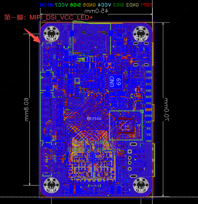
Page 11 of the panel datasheet identifies its pin 1, also LED+. With the orientations shown, a same-side-contact cable connects these pins correctly.
Configure the Panel
Open the Taishan Pi user device tree, linux/kernel/arch/arm64/boot/dts/tspi-rk3566-user-v10-linux.dts, and locate the included MIPI configuration.
diff --git a/arch/arm64/boot/dts/rockchip/tspi-rk3566-user-v10-linux.dts b/arch/arm64/boot/dts/rockchip/tspi-rk3566-user-v10-linux.dts
index 97da688286b2..c80eda51d362 100755
--- a/arch/arm64/boot/dts/rockchip/tspi-rk3566-user-v10-linux.dts
+++ b/arch/arm64/boot/dts/rockchip/tspi-rk3566-user-v10-linux.dts
@@ -33,10 +33,10 @@
 // #include "tspi-rk3566-edp-v10.dtsi"

 //【开/关】mipi 显示屏幕配置,用户可以基于此复制自己的屏幕,注意EDP与MIPI屏幕互斥,因为共用了VOP如果需要同显自行修改
-// #include "tspi-rk3566-dsi-v10.dtsi"
+#include "tspi-rk3566-dsi-v10.dtsi"

 //【开/关】HDMI 显示屏幕配置,里面内容几乎可以不用动,如果不需要hdmi显示直接注释掉即可
-#include "tspi-rk3566-hdmi-v10.dtsi"
+// #include "tspi-rk3566-hdmi-v10.dtsi"

 //【开/关】摄像头 目前视频的是ov5659
#include "tspi-rk3566-csi-v10.dtsi"DSI Device Tree
The MIPI configuration is in tspisdk/kernel/arch/arm64/boot/dts/rockchip/tspi-rk3566-dsi-v10.dtsi. This example mainly changes lines 49, 73, and 90–98. The following sections explain the nodes; beginners can first follow the panel parameter example.
/ {
        backlight: backlight {
                compatible = "pwm-backlight";
                pwms = <&pwm5 0 25000 0>;
                brightness-levels = <...>; // 亮度级别
                default-brightness-level = <255>; // 默认亮度级别
        };
};

&pwm5 {
        status = "okay"; // PWM控制器状态
};

&pinctrl {
        dsi1 {
                dsi1_rst_gpio: dsi1-rst-gpio {
                        rockchip,pins = <3 RK_PC1 RK_FUNC_GPIO &pcfg_pull_none>; // DSI1复位引脚配置
                };
        };
};
/*
 * video_phy1 需要在启用 dsi1 时启用
 */
&dsi1 {
        status = "okay"; // DSI1控制器状态
};
//注意我们前面有讲到rk3566有两个vop,我们这里就是来链接vop的,你可以选择1或者0这里我们选择0
&dsi1_in_vp0 {
        status = "okay"; // 0状态
};

&dsi1_in_vp1 {
        status = "disabled"; // DSI1输入虚拟通道1状态
};

&video_phy1 {
        status = "okay"; // 视频 PHY1状态
};

&route_dsi1 {
        status = "okay"; // 路由 DSI1状态
        connect = <&vp0_out_dsi1>; // 连接到 DSI1输入虚拟通道0
};

// 默认 8 寸 800x1280 分辨率
&dsi1 {
        status = "okay"; // DSI1控制器状态
        rockchip,lane-rate = <480>; // DSI1通道速率

        dsi1_panel: panel@0 {
                status = "okay"; // DSI1面板状态
                compatible = "simple-panel-dsi";

                reset-gpios = <&gpio3 RK_PC1 GPIO_ACTIVE_LOW>; // 复位GPIO引脚配置
                pinctrl-names = "default";
                pinctrl-0 = <&dsi1_rst_gpio>;

                reg = <0>;
                backlight = <&backlight>; // 关联背光控制节点

                reset-delay-ms = <10>;
                enable-delay-ms = <120>;
                prepare-delay-ms = <20>;
                unprepare-delay-ms = <20>;
                disable-delay-ms = <50>;

                dsi,flags = <(MIPI_DSI_MODE_VIDEO | MIPI_DSI_MODE_VIDEO_BURST |
                        MIPI_DSI_MODE_LPM | MIPI_DSI_MODE_EOT_PACKET)>; // DSI模式标志
                dsi,format = <MIPI_DSI_FMT_RGB888>; // DSI格式
                dsi,lanes  = <4>; // DSI通道数

                panel-init-sequence = [
                        15 00 02 E0 00
                        15 00 02 E1 93
                        //.............
                        05 fa 01 11
                        05 32 01 29
                ]; // 面板初始化序列

                panel-exit-sequence = [
                        05 00 01 28
                        05 00 01 10
                ]; // 面板退出序列

                disp_timings1: display-timings {
                        native-mode = <&dsi1_timing0>;

                        dsi1_timing0: timing0 {
                                clock-frequency = <66000000>; // 时钟频率
                                hactive = <800>; // 水平像素
                                vactive = <1280>; // 垂直像素
                                hfront-porch = <18>; // 水平前廊
                                hsync-len = <12>; // 水平同步长度
                                hback-porch = <18>; // 水平后廊
                                vfront-porch = <24>; // 垂直前廊
                                vsync-len = <4>; // 垂直同步长度
                                vback-porch = <12>; // 垂直后廊
                                hsync-active = <0>; // 水平同步极性激活
                                vsync-active = <0>; // 垂直同步极性激活
                                de-active = <0>; // 数据使能极性激活
                                pixelclk-active = <1>; // 像素时钟极性激活
                        };
                };

                ports {
                        #address-cells = <1>;
                        #size-cells = <0>;

                        port@0 {
                                reg = <0>;
                                panel_in_dsi1: endpoint {
                                        remote-endpoint = <&dsi1_out_panel>;
                                };
                        };
                };
        };

        ports {
                #address-cells = <1>;
                #size-cells = <0>;

                port@1 {
                        reg = <1>;
                        dsi1_out_panel: endpoint {
                                remote-endpoint = <&panel_in_dsi1>;
                        };
                };
        };
};Backlight
The backlight node references PWM5, and the MIPI panel node references that backlight. Enabling the PWM5 controller lets PWM5 control the panel brightness.
/ {
        backlight: backlight {
                compatible = "pwm-backlight";
                pwms = <&pwm5 0 25000 0>;
                brightness-levels = <...>; // 亮度级别
                default-brightness-level = <255>; // 默认亮度级别
        };
};
&pwm5 {
        status = "okay"; // PWM控制器状态
};
&dsi1 {
        //...........
        dsi1_panel: panel@0 {
                //...........
                backlight = <&backlight>; // 关联背光控制节点
                //...........
        };
        //...........
};GPIO0_C4_d supports PWM5. Check the datasheet or the PWM5 pinctrl definitions in .tspi-rk3566-user-v10.dtb.dts.tmp. This pin connects to the backlight driver's enable input. The _d and _u suffixes indicate default pull-down and pull-up states. SY7201ABC is disabled by a low level, so this design uses GPIO0_C4_d to keep the backlight off before software takes control.
PWM5_LCD_BL connects to the backlight enable input.
Reset Pin
The abbreviated device tree below enables the GPIO controller, assigns the panel reset pin, and sets reset delays.
&pinctrl {
        dsi1 {
                dsi1_rst_gpio: dsi1-rst-gpio {
                        rockchip,pins = <3 RK_PC1 RK_FUNC_GPIO &pcfg_pull_none>; // DSI1复位引脚配置
                };
        };
};
// 默认 8 寸 800x1280 分辨率
&dsi1 {
        dsi1_panel: panel@0 {
                reset-gpios = <&gpio3 RK_PC1 GPIO_ACTIVE_LOW>; // 复位GPIO引脚配置
                pinctrl-names = "default";
                pinctrl-0 = <&dsi1_rst_gpio>;
                reset-delay-ms = <10>;    //设置复位延时,这个一般可以在屏幕数据手册里面找到,一般容差都很宽
        };
};The example uses GPIO3_C1_d as the reset GPIO. Its power domain is VCC_3V3.
The note on page 7 relates RESET voltage to VDDIO. Pin 27 (RESET) connects to GPIO3_C1_d, which outputs 3.3 V when high, so pin 29 (logic power) connects to VCC_3V3.
Enable DSI1
RK3566 has DSI0 and DSI1. Taishan Pi exposes DSI1, so enable the DSI1-related nodes below.
/*
 * video_phy1 需要在启用 dsi1 时启用
 */
&dsi1 {
        status = "okay"; // DSI1控制器状态
};
//注意我们前面有讲到rk3566有两个vop,我们这里就是来链接vop的,你可以选择1或者0这里我们选择0
//mipi接口也是有两个的我们这里选择dis1,链接到vp0
&dsi1_in_vp0 {
        status = "okay"; // 0状态
};

&dsi1_in_vp1 {
        status = "disabled"; // DSI1输入虚拟通道1状态
};

&video_phy1 {
        status = "okay"; // 视频 PHY1状态
};

&route_dsi1 {
        status = "okay"; // 路由 DSI1状态
        connect = <&vp0_out_dsi1>; // 连接到 DSI1输入虚拟通道0
};

// 默认 8 寸 800x1280 分辨率
&dsi1 {
};DSI1 Data Rate
The data rate can be specified manually. This example leaves the setting commented out so the driver calculates it.
&dsi1
        //rockchip,lane-rate = <480>; // DSI1通道速率
};Data Lane Count
Set the lane count to match the panel: four for four differential data pairs, or two for two pairs.
&dsi1 {
    dsi1_panel: panel@0 {
        dsi,lanes  = <4>;
    };
};The panel above has four differential data pairs, so set dsi,lanes to 4.
The later 3.1-inch, 480 × 800 panel has two differential data pairs, so its lane count is 2.
Initialization Sequence
The initialization sequence configures the panel controller. A wrong value can prevent any image from appearing. Ask the supplier for a tested sequence, preferably for RK3566. Although register values can be derived from the controller datasheet, there are many settings and errors are easy to make. Some panels have a built-in configuration and do not require a sequence from the host.
&dsi1 {
    dsi1_panel: panel@0 {
        /*初始化序列*/
        panel-init-sequence = [
            15 00 02 E0 00
            15 00 02 E1 93
            /*...........*/
            05 fa 01 11
            05 32 01 29
        ];
        /*退出序列*/
        panel-exit-sequence = [
            05 00 01 28
            05 00 01 10
        ];
    };
};Sequence Format
Rockchip uses the sequence format below. Suppliers may provide the same data in another format; understanding the fields lets you convert it.
[packet type][delay][payload length][panel initialization data * n]
Example:
39 00 06 FF 77 01 00 00 11
15 00 02 E0 00
05 00 01 28Packet Types
The examples use packet types 39, 15, and 05. See page 60 of Mipi-DSI-specification-v1-3.pdf for more types. This tutorial covers these common cases. Further reading: https://blog.csdn.net/u013606261/article/details/112535270
0x39
0x39 DCS Long Write/write_LUT Command Packet carries a DCS long-write command or lookup-table data. For example: 39 00 06 FF 77 01 00 00 11
39: DCS long-write packet type.00: No additional delay.06: Six payload bytes follow.FF 77 01 00 00 11: Payload.
[DCS指令][发送延时][描述数据长度受DCS指令影响][MIPI屏初始化数据个数由前面的数据长度决定]
39 00 06 FF 77 01 00 00 110x15
0x15 DCS Short WRITE, 1 parameter sends a command with one parameter. For example: 15 00 02 E0 00
15: DCS short-write packet type with one parameter.00: No additional delay.02: Two payload bytes, comprising the command and its parameter.E0 00: Payload.
[DCS指令][发送延时][描述数据长度受DCS指令影响][MIPI屏初始化数据个数由前面的数据长度决定]
15 00 02 E0 000x05
0x05 DCS Short WRITE, no parameters sends a command without parameters.
For example:05 00 01 28
05: DCS short-write packet type with no parameters.00: No additional delay.01: One payload byte, containing the command.28: Command byte.
[DCS指令][发送延时][描述数据长度受DCS指令影响][MIPI屏初始化数据个数由前面的数据长度决定]
05 00 01 28timings
This property works as in the eDP example.
Panel Timing
Enable DSI1 and the Backlight
First enable the backlight. Then configure the panel timings from its datasheet and the initialization sequence from its supplier.
&dsi1 {
    status = "okay";
    rockchip,lane-rate = <500>;
    dsi1_panel: panel@0 {
        status = "okay";
        compatible = "simple-panel-dsi";
        reset-gpios = <&gpio3 RK_PC1 GPIO_ACTIVE_LOW>;
        pinctrl-names = "default";
        pinctrl-0 = <&dsi1_rst_gpio>;
        reg = <0>;
        backlight = <&backlight>;
        reset-delay-ms = <30>;
        enable-delay-ms = <100>;
        prepare-delay-ms = <20>;
        unprepare-delay-ms = <20>;
        disable-delay-ms = <20>;
        init-delay-ms = <10>;
        dsi,flags = <(MIPI_DSI_MODE_VIDEO | MIPI_DSI_MODE_VIDEO_BURST |
            MIPI_DSI_MODE_LPM | MIPI_DSI_MODE_EOT_PACKET)>;
        dsi,format = <MIPI_DSI_FMT_RGB888>;
        dsi,lanes  = <4>;
        panel-init-sequence = [
        ];

        panel-exit-sequence = [
        ];

        disp_timings1: display-timings {
            native-mode = <&dsi1_timing0>;
            dsi1_timing0: timing0 {
                clock-frequency = <0>;
                hactive = <0>;
                vactive = <0>;
                hfront-porch = <0>;
                hsync-len = <0>;
                hback-porch = <0>;
                vfront-porch = <0>;
                vsync-len = <0>;
                vback-porch = <0>;
                hsync-active = <0>;
                vsync-active = <0>;
                de-active = <0>;
                pixelclk-active = <0>;
            };
        };

        ports {
            #address-cells = <1>;
            #size-cells = <0>;

            port@0 {
                reg = <0>;
                panel_in_dsi1: endpoint {
                    remote-endpoint = <&dsi1_out_panel>;
                };
            };
        };
    };

    ports {
        #address-cells = <1>;
        #size-cells = <0>;

        port@1 {
            reg = <1>;
            dsi1_out_panel: endpoint {
                remote-endpoint = <&panel_in_dsi1>;
            };
        };
    };

};timings
Fill in the timings using the supplier's reference or page 9 of the datasheet.
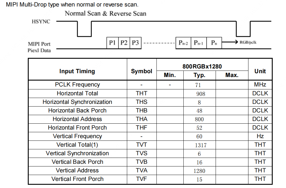
Copy the relevant datasheet values into timings. The annotations below show the correspondence.
disp_timings1: display-timings {
    native-mode = <&dsi1_timing0>;
    dsi1_timing0: timing0 {
        clock-frequency = <71000000>;   //PCLK Frequency
        hactive = <800>;                //Horizontal Address
        vactive = <1280>;               //Vertical Address
        hfront-porch = <52>;            //Horizontal Front Porch
        hsync-len = <8>;                //Horizontal Synchronization
        hback-porch = <48>;             //Horizontal Back Porch
        vfront-porch = <15>;            //Vertical Front Porch
        vsync-len = <6>;                //Vertical Synchronization
        vback-porch = <16>;             //Vertical Back Porch
        hsync-active = <0>;
        vsync-active = <0>;
        de-active = <0>;
        pixelclk-active = <0>;
    };
}Convert the Initialization Sequence
The supplier's sequence is available with the files linked above. Its format differs from Rockchip's, so convert the format while keeping the command data unchanged.
{0xFF,3,{0x98,0x81,0x03}},//PAGE3
{0x01,1,{0x00}},
{0x02,1,{0x00}},
{0x03,1,{0x53}},
{0x04,1,{0x53}},
{0x05,1,{0x13}},
{0x06,1,{0x04}},
{0x07,1,{0x02}},
{0x08,1,{0x02}},
{0x09,1,{0x00}},
{0x0a,1,{0x00}},
{0x0b,1,{0x00}},
{0x0c,1,{0x00}},
{0x0d,1,{0x00}},
{0x0e,1,{0x00}},
{0x0f,1,{0x00}},
{0x10,1,{0x00}},
{0x11,1,{0x00}},
{0x12,1,{0x00}},
{0x13,1,{0x00}},
{0x14,1,{0x00}},
{0x15,1,{0x00}},
{0x16,1,{0x00}},
{0x17,1,{0x00}},
{0x18,1,{0x00}},
{0x19,1,{0x00}},
{0x1a,1,{0x00}},
{0x1b,1,{0x00}},
{0x1c,1,{0x00}},
{0x1d,1,{0x00}},
{0x1e,1,{0xc0}},
{0x1f,1,{0x00}},
{0x20,1,{0x02}},
{0x21,1,{0x09}},
{0x22,1,{0x00}},
{0x23,1,{0x00}},
{0x24,1,{0x00}},
{0x25,1,{0x00}},
{0x26,1,{0x00}},
{0x27,1,{0x00}},
{0x28,1,{0x55}},
{0x29,1,{0x03}},
{0x2a,1,{0x00}},
{0x2b,1,{0x00}},
{0x2c,1,{0x00}},
{0x2d,1,{0x00}},
{0x2e,1,{0x00}},
{0x2f,1,{0x00}},
{0x30,1,{0x00}},
{0x31,1,{0x00}},
{0x32,1,{0x00}},
{0x33,1,{0x00}},
{0x34,1,{0x00}},
{0x35,1,{0x00}},
{0x36,1,{0x00}},
{0x37,1,{0x00}},
{0x38,1,{0x3C}},
{0x39,1,{0x00}},
{0x3a,1,{0x00}},
{0x3b,1,{0x00}},
{0x3c,1,{0x00}},
{0x3d,1,{0x00}},
{0x3e,1,{0x00}},
{0x3f,1,{0x00}},
{0x40,1,{0x00}},
{0x41,1,{0x00}},
{0x42,1,{0x00}},
{0x43,1,{0x00}},
{0x44,1,{0x00}},
//{0x45,1,{0x00}},

{0x50,1,{0x01}},
{0x51,1,{0x23}},
{0x52,1,{0x45}},
{0x53,1,{0x67}},
{0x54,1,{0x89}},
{0x55,1,{0xab}},
{0x56,1,{0x01}},
{0x57,1,{0x23}},
{0x58,1,{0x45}},
{0x59,1,{0x67}},
{0x5a,1,{0x89}},
{0x5b,1,{0xab}},
{0x5c,1,{0xcd}},
{0x5d,1,{0xef}},

{0x5e,1,{0x01}},
{0x5f,1,{0x0A}},    //FW_CGOUT_L[1] RESE_ODD
{0x60,1,{0x02}},     //FW_CGOUT_L[2] VSSG_ODD
{0x61,1,{0x02}},     //FW_CGOUT_L[3] VSSG_ODD
{0x62,1,{0x08}},     //FW_CGOUT_L[4] STV2_ODD
{0x63,1,{0x15}},     //FW_CGOUT_L[5] VDD2_ODD
{0x64,1,{0x14}},     //FW_CGOUT_L[6] VDD1_ODD
{0x65,1,{0x02}},     //FW_CGOUT_L[7]
{0x66,1,{0x11}},     //FW_CGOUT_L[8] CK11
{0x67,1,{0x10}},     //FW_CGOUT_L[9] CK9
{0x68,1,{0x02}},     //FW_CGOUT_L[10]
{0x69,1,{0x0F}},     //FW_CGOUT_L[11] CK7
{0x6a,1,{0x0E}},     //FW_CGOUT_L[12] CK5
{0x6b,1,{0x02}},     //FW_CGOUT_L[13]
{0x6c,1,{0x0D}},     //FW_CGOUT_L[14] CK3
{0x6d,1,{0x0C}},     //FW_CGOUT_L[15] CK1
{0x6e,1,{0x06}},     //FW_CGOUT_L[16] STV1_ODD
{0x6f,1,{0x02}},     //FW_CGOUT_L[17]
{0x70,1,{0x02}},     //FW_CGOUT_L[18]
{0x71,1,{0x02}},     //FW_CGOUT_L[19]
{0x72,1,{0x02}},     //FW_CGOUT_L[20]
{0x73,1,{0x02}},     //FW_CGOUT_L[21]
{0x74,1,{0x02}},     //FW_CGOUT_L[22]

{0x75,1,{0x0A}},     //BW_CGOUT_L[1]   RESE_ODD
{0x76,1,{0x02}},     //BW_CGOUT_L[2]   VSSG_ODD
{0x77,1,{0x02}},     //BW_CGOUT_L[3]   VSSG_ODD
{0x78,1,{0x06}},     //BW_CGOUT_L[4]   STV2_ODD
{0x79,1,{0x15}},     //BW_CGOUT_L[5]   VDD2_ODD
{0x7a,1,{0x14}},     //BW_CGOUT_L[6]   VDD1_ODD
{0x7b,1,{0x02}},     //BW_CGOUT_L[7]
{0x7c,1,{0x10}},     //BW_CGOUT_L[8]   CK11
{0x7d,1,{0x11}},     //BW_CGOUT_L[9]   CK9
{0x7e,1,{0x02}},     //BW_CGOUT_L[10]
{0x7f,1,{0x0C}},     //BW_CGOUT_L[11]  CK7
{0x80,1,{0x0D}},     //BW_CGOUT_L[12]  CK5
{0x81,1,{0x02}},     //BW_CGOUT_L[13]
{0x82,1,{0x0E}},     //BW_CGOUT_L[14]  CK3
{0x83,1,{0x0F}},     //BW_CGOUT_L[15]  CK1
{0x84,1,{0x08}},     //BW_CGOUT_L[16]  STV1_ODD
{0x85,1,{0x02}},     //BW_CGOUT_L[17]
{0x86,1,{0x02}},     //BW_CGOUT_L[18]
{0x87,1,{0x02}},     //BW_CGOUT_L[19]
{0x88,1,{0x02}},     //BW_CGOUT_L[20]
{0x89,1,{0x02}},     //BW_CGOUT_L[21]
{0x8A,1,{0x02}},     //BW_CGOUT_L[22]


{0xFF,3,{0x98,0x81,0x04}},//PAGE4
//{0x00,1,{0x00}},//3L  打开此行
//{0x2F,1,{0x01}},//BIST
{0x3B,1,{0xC0}},    // ILI4003D sel
{0x6C,1,{0x15}},
{0x6E,1,{0x30}},     //VGH 16V
{0x6F,1,{0x55}},     //Pump ratio VGH=VSPX4 VGL=VSNX4
{0x3A,1,{0x24}},
{0x8D,1,{0x1F}},
{0x87,1,{0xBA}},
{0x26,1,{0x76}},
{0xB2,1,{0xD1}},
{0xB5,1,{0x07}},
{0x35,1,{0x1F}},
{0x88,1,{0x0B}},
{0x21,1,{0x30}},


{0xFF,3,{0x98,0x81,0x01}},//PAGE1
{0x22,1,{0x0A}},
{0x31,1,{0x09}},
{0x40,1,{0x33}},
{0x53,1,{0x37}},
{0x55,1,{0x38}},
{0x50,1,{0x95}},
{0x51,1,{0x95}},
{0x60,1,{0x30}},

{0xA0,1,{0x0F}},        //VP255Gamma P
{0xA1,1,{0x17}},               //VP251
{0xA2,1,{0x22}},               //VP247
{0xA3,1,{0x19}},              //VP243
{0xA4,1,{0x15}},               //VP239
{0xA5,1,{0x28}},               //VP231
{0xA6,1,{0x1C}},               //VP219
{0xA7,1,{0x1C}},               //VP203
{0xA8,1,{0x78}},               //VP175
{0xA9,1,{0x1C}},               //VP144
{0xAA,1,{0x28}},               //VP111
{0xAB,1,{0x69}},               //VP80
{0xAC,1,{0x1A}},               //VP52
{0xAD,1,{0x19}},               //VP36
{0xAE,1,{0x4B}},               //VP24
{0xAF,1,{0x22}},               //VP16
{0xB0,1,{0x2A}},               //VP12
{0xB1,1,{0x4B}},               //VP8
{0xB2,1,{0x6B}},               //VP4
{0xB3,1,{0x3F}},               //VP0

{0xC0,1,{0x01}},         //VN255 GAMMA N
{0xC1,1,{0x17}},               //VN251
{0xC2,1,{0x22}},               //VN247
{0xC3,1,{0x19}},              //VN243
{0xC4,1,{0x15}},               //VN239
{0xC5,1,{0x28}},               //VN231
{0xC6,1,{0x1C}},               //VN219
{0xC7,1,{0x1D}},               //VN203
{0xC8,1,{0x78}},               //VN175
{0xC9,1,{0x1C}},               //VN144
{0xCA,1,{0x28}},               //VN111
{0xCB,1,{0x69}},               //VN80
{0xCC,1,{0x1A}},               //VN52
{0xCD,1,{0x19}},               //VN36
{0xCE,1,{0x4B}},               //VN24
{0xCF,1,{0x22}},               //VN16
{0xD0,1,{0x2A}},               //VN12
{0xD1,1,{0x4B}},               //VN8
{0xD2,1,{0x6B}},               //VN4
{0xD3,1,{0x3F}},               //VN0

{0xFF,3,{0x98,0x81,0x00}},//PAGE0
//{0x35,1,{0x00}},               //TE OUT
{0x11,0,{0x00}},        //sleep out
{REGFLAG_DELAY, 120, {}},
{0x29,0,{0x00}},        //display on
{REGFLAG_DELAY, 5, {}},The reference sequence uses these two formats: Format 1: [address] [length] [data] For example:
[地址]   [长度]   [数据]
{0xFF,     3,  {0x98,0x81,0x03}},
{0x01, 1, {0x00}},Format 2: [delay type] [delay time] [empty] For example:
[延时类型]        [延时时间]    [空值]
{REGFLAG_DELAY, 120, {}},The Taishan Pi RK3566 sequence format is: Format: [packet type] [delay] [payload length] [panel initialization payload] Convert line 1:
转换前
{0xFF,3,{0x98,0x81,0x03}},//PAGE3Packet type: The source command has three parameter bytes, so use long write 0x39.
Delay: No delay follows, so use 00 ms.
Payload length: The command address and three parameter bytes total four bytes.
Payload: Include the address followed by its data.
转换后
39 00 04 FF 98 81 03Convert line 2:
转换前
{0x01,1,{0x00}},Packet type: The command has one parameter byte, so use short write 0x15.
Delay: No delay follows, so use 00 ms.
Payload length: The address and one parameter total two bytes.
Payload: Include the address followed by its data.
After Conversion
15 00 02 01 00Lines 207-208 conversion:
转换前
{0x11,0,{0x00}},        //sleep out
{REGFLAG_DELAY, 120, {}},Packet type: The command has no parameters, so use short write 0x05.
Delay: The next line specifies 120 ms, encoded as 0x78.
Payload length: One byte, containing the command address.
Payload: Only the address, because there are no parameters.
转换后
05 78 01 11The complete converted sequence is:
        panel-init-sequence = [
            39 00 04 FF 98 81 03
            15 00 02 01 00
            15 00 02 02 00
            15 00 02 03 53
            15 00 02 04 53
            15 00 02 05 13
            15 00 02 06 04
            15 00 02 07 02
            15 00 02 08 02
            15 00 02 09 00
            15 00 02 0a 00
            15 00 02 0b 00
            15 00 02 0c 00
            15 00 02 0d 00
            15 00 02 0e 00
            15 00 02 0f 00
            15 00 02 10 00
            15 00 02 11 00
            15 00 02 12 00
            15 00 02 13 00
            15 00 02 14 00
            15 00 02 15 00
            15 00 02 16 00
            15 00 02 17 00
            15 00 02 18 00
            15 00 02 19 00
            15 00 02 1a 00
            15 00 02 1b 00
            15 00 02 1c 00
            15 00 02 1d 00
            15 00 02 1e c0
            15 00 02 1f 00
            15 00 02 20 02
            15 00 02 21 09
            15 00 02 22 00
            15 00 02 23 00
            15 00 02 24 00
            15 00 02 25 00
            15 00 02 26 00
            15 00 02 27 00
            15 00 02 28 55
            15 00 02 29 03
            15 00 02 2a 00
            15 00 02 2b 00
            15 00 02 2c 00
            15 00 02 2d 00
            15 00 02 2e 00
            15 00 02 2f 00
            15 00 02 30 00
            15 00 02 31 00
            15 00 02 32 00
            15 00 02 33 00
            15 00 02 34 00
            15 00 02 35 00
            15 00 02 36 00
            15 00 02 37 00
            15 00 02 38 3C
            15 00 02 39 00
            15 00 02 3a 00
            15 00 02 3b 00
            15 00 02 3c 00
            15 00 02 3d 00
            15 00 02 3e 00
            15 00 02 3f 00
            15 00 02 40 00
            15 00 02 41 00
            15 00 02 42 00
            15 00 02 43 00
            15 00 02 44 00

            15 00 02 50 01
            15 00 02 51 23
            15 00 02 52 45
            15 00 02 53 67
            15 00 02 54 89
            15 00 02 55 ab
            15 00 02 56 01
            15 00 02 57 23
            15 00 02 58 45
            15 00 02 59 67
            15 00 02 5a 89
            15 00 02 5b ab
            15 00 02 5c cd
            15 00 02 5d ef

            15 00 02 5e 01
            15 00 02 5f 0A
            15 00 02 60 02
            15 00 02 61 02
            15 00 02 62 08
            15 00 02 63 15
            15 00 02 64 14
            15 00 02 65 02
            15 00 02 66 11
            15 00 02 67 10
            15 00 02 68 02
            15 00 02 69 0F
            15 00 02 6a 0E
            15 00 02 6b 02
            15 00 02 6c 0D
            15 00 02 6d 0C
            15 00 02 6e 06
            15 00 02 6f 02
            15 00 02 70 02
            15 00 02 71 02
            15 00 02 72 02
            15 00 02 73 02
            15 00 02 74 02

            15 00 02 75 0A
            15 00 02 76 02
            15 00 02 77 02
            15 00 02 78 06
            15 00 02 79 15
            15 00 02 7a 14
            15 00 02 7b 02
            15 00 02 7c 10
            15 00 02 7d 11
            15 00 02 7e 02
            15 00 02 7f 0C
            15 00 02 80 0D
            15 00 02 81 02
            15 00 02 82 0E
            15 00 02 83 0F
            15 00 02 84 08
            15 00 02 85 02
            15 00 02 86 02
            15 00 02 87 02
            15 00 02 88 02
            15 00 02 89 02
            15 00 02 8A 02

            39 00 04 FF 98 81 04
            //15 00 02 00 00  //
            // 15 00 02 2F 01   //bist 用户调试,屏幕会闪演示测试
            15 00 02 3B C0
            15 00 02 6C 15
            15 00 02 6E 30
            15 00 02 6F 55
            15 00 02 3A 24
            15 00 02 8D 1F
            15 00 02 87 BA
            15 00 02 26 76
            15 00 02 B2 D1
            15 00 02 B5 07
            15 00 02 35 1F
            15 00 02 88 0B
            15 00 02 21 09

            39 00 04 FF 98 81 01
            15 00 02 22 0A
            15 00 02 31 09
            15 00 02 40 33
            15 00 02 53 37
            15 00 02 55 38
            15 00 02 50 95
            15 00 02 51 95
            15 00 02 60 30

            15 00 02 A0 0F
            15 00 02 A1 17
            15 00 02 A2 22
            15 00 02 A3 19
            15 00 02 A4 15
            15 00 02 A5 28
            15 00 02 A6 1C
            15 00 02 A7 1C
            15 00 02 A8 78
            15 00 02 A9 1C
            15 00 02 AA 28
            15 00 02 AB 69
            15 00 02 AC 1A
            15 00 02 AD 19
            15 00 02 AE 4B
            15 00 02 AF 22
            15 00 02 B0 2A
            15 00 02 B1 4B
            15 00 02 B2 6B
            15 00 02 B3 3F

            15 00 02 C0 01
            15 00 02 C1 17
            15 00 02 C2 22
            15 00 02 C3 19
            15 00 02 C4 15
            15 00 02 C5 28
            15 00 02 C6 1C
            15 00 02 C7 1D
            15 00 02 C8 78
            15 00 02 C9 1C
            15 00 02 CA 28
            15 00 02 CB 69
            15 00 02 CC 1A
            15 00 02 CD 19
            15 00 02 CE 4B
            15 00 02 CF 22
            15 00 02 D0 2A
            15 00 02 D1 4B
            15 00 02 D2 6B
            15 00 02 D3 3F
            39 00 04 FF 98 81 00
            05 78 01 11
            05 05 01 29
];Replace the timings and initialization sequence in your Android or Linux source with these values, then build and flash to test this panel.
Patch
Linux Patch
Download tspi_Linux_mipi800x1280_patch.zip
📌 Find it under 下载中心 → 百度网盘(立创·泰山派开发板资料) → 第09章.【立创·泰山派】项目案例 → 【智能小手机】项目资料 → 5.屏幕选型与调试 → MIPI屏资料 → 代码补丁 → tspi_Linux_mipi800x1280_patch.zip.
The Android patch also includes touchscreen changes. For MIPI display output alone, only tspi-rk3566-dsi-v10.dtsi needs changing.
Download tspi_Android_mipi800x1280_patch.zip
📌 Find it under 下载中心 → 百度网盘(立创·泰山派开发板资料) → 第09章.【立创·泰山派】项目案例 → 【智能小手机】项目资料 → 5.屏幕选型与调试 → MIPI屏资料 → 代码补丁 → tspi_Android_mipi800x1280_patch.zip.
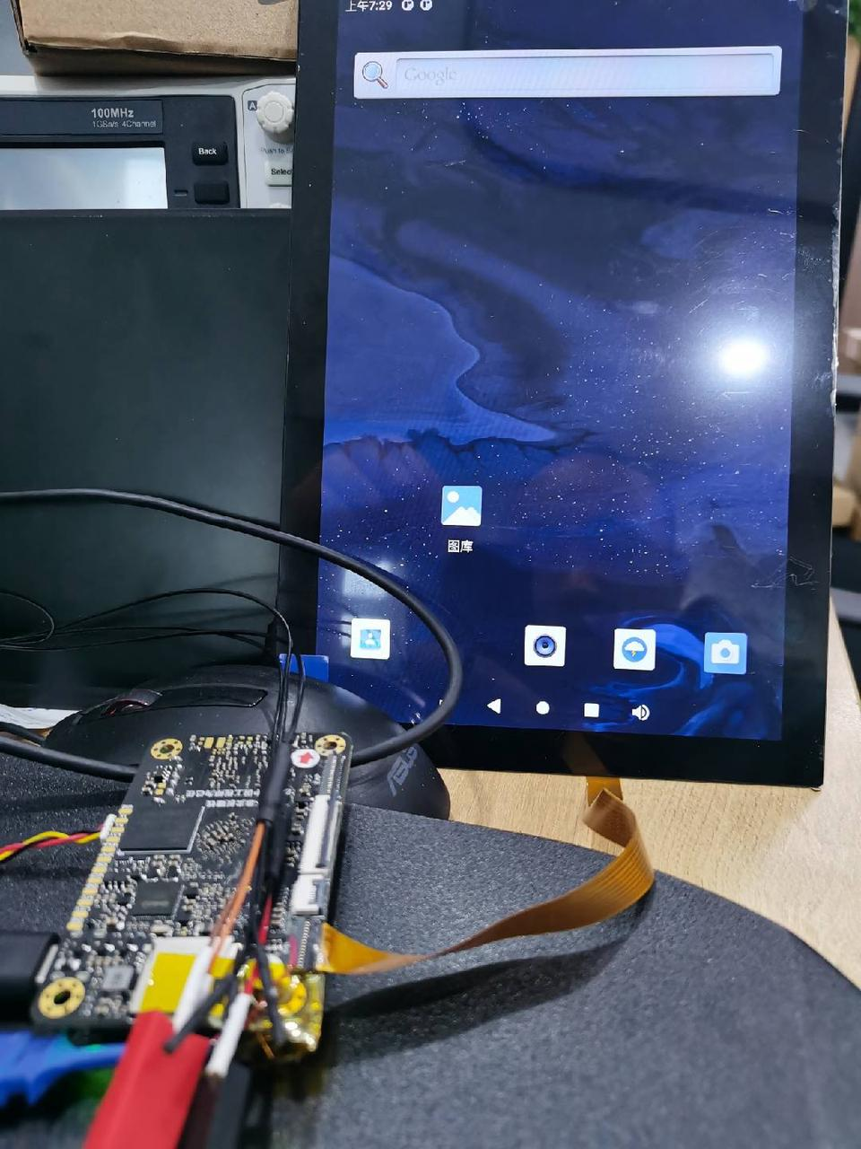
Test the Display
Build and flash the kernel as described in Build the SDK.
Understand the Sequence
The sequence writes configuration registers in the panel controller, much like an I²C or SPI display driver. To understand the values, identify the controller and read its datasheet. Page 4 of the panel datasheet identifies its controller as ILI9881C.
Controller datasheet:
Download: ILI9881C-MIIPI-DataSheet.pdf
📌 Find it under 下载中心 → 百度网盘(立创·泰山派开发板资料) → 第09章.【立创·泰山派】项目案例 → 【智能小手机】项目资料 → 5.屏幕选型与调试 → MIPI屏资料 → 屏幕资料 → ILI9881C-MIIPI-DataSheet.pdf.
Command descriptions start in Chapter 5 on page 113.
The table below lists register pages and their selection commands. 39 00 04 FF 98 81 XX selects a page. For example:
39 00 04 FF 98 81 03 //进入Page3页
/*...页面3相关寄存器操作....*/
39 00 04 FF 98 81 04 //进入Page4页
/*...页面4相关寄存器操作....*/
39 00 04 FF 98 81 01 //进入Page1页
/*...页面1相关寄存器操作....*/
39 00 04 FF 98 81 00  //进入Page0页
/*...页面0相关寄存器操作....*/After selecting a page, the sequence writes registers on that page. The example selects page 3, then writes registers 0x01–0x8A (the screenshot is shortened).
See ILI9881C datasheet page 115, section 5.2.4.
Each register has a specific function. For example, writing register 0x2F on page 4 enables a display test.
See ILI9881C datasheet page 118, section 5.2.5, BIST Mode Function.
Page 236, section 5.7.6, describes BIST Mode Function. This sequence writes 0x01 to 0x2F, setting FRM_EN to 1 and enabling the built-in self-test (BIST).
Build, flash, and test:
Next, change the sequence to mirror the MIPI display:
See ILI9881C datasheet page 109, section 5.2.1, Memory Access.
Page 145, section 5.3.21, describes Memory Access Control. This sequence writes 0x02 to 0x36, changing the SS bit and display direction.
Result: